The Photonic Dilemma
Why the Future of AI May Depend on Manufacturing, Not Physics
The invisible limit of artificial intelligence
While the world marvels at increasingly human-like responses from artificial intelligence, engineers in the cleanrooms of Silicon Valley are grappling with a stubborn law of physics: copper is running out of road. The electrical cables and interconnects that stitch together today’s data centers are approaching their thermal and bandwidth limits. As AI models scale into the trillions of parameters, the challenge is no longer simply how fast a processor can compute—but how fast information can move between thousands of them.
In the sprawling infrastructure behind modern AI systems, the bottleneck has shifted. Graphics processors may perform trillions of calculations per second, but those calculations are useless if data cannot flow quickly enough between chips, racks and clusters. The result is a growing engineering crisis quietly unfolding behind the scenes of the AI boom.
It is here that an alternative technology—long studied but rarely deployed at scale—has returned to the center of attention: silicon photonics. Instead of sending electrical signals through copper wires, photonic systems use light to transmit information through microscopic optical pathways etched into chips.
“The bottleneck for AI is no longer the compute itself, but the ability to move data between the compute elements. Silicon photonics is the only path to scale the bandwidth density required for the next generation of LLMs.”
Mark Wade
CEO & Co-founder, Ayar Labs
Source: AI Hardware & Edge AI Summit
For Wade and others working at the frontier of AI hardware, the implication is clear: the future of artificial intelligence may hinge less on algorithmic breakthroughs than on the physical infrastructure that moves data through machines.
The Power Wall
The modern AI data center is an engineering marvel—rows of racks filled with GPUs, accelerators and high-speed networking equipment working together as a single computational organism. But the very architecture that allows AI systems to scale is now running into an unavoidable physical constraint.
As models grow larger, they must be distributed across more processors. Each processor must constantly exchange information with its neighbors. This process, known as interconnect communication, increasingly dominates the energy consumption of AI systems.
Copper interconnects, which have served computing well for decades, are reaching their practical limits. Electrical signals traveling through copper wires generate heat and encounter resistance, leading to energy losses and cooling challenges.
“We are approaching the ‘Power Wall’. We can build bigger GPUs, but we cannot feed them enough power or cool them efficiently using traditional copper interconnects. Light is the only way out of this thermal trap.”
Jensen Huang
CEO, NVIDIA
Source: GTC Keynote
The warning reflects a broader shift in how engineers think about computing systems. For much of the past half-century, progress depended primarily on making processors faster. Today, the limiting factor is increasingly the infrastructure connecting those processors.
In other words, the future of AI may depend not just on computation, but on communication.
Enter Silicon Photonics
Silicon photonics offers a compelling solution. By transmitting data using photons instead of electrons, optical communication can dramatically increase bandwidth while reducing energy consumption.
The idea itself is not new. Optical fibers have carried internet traffic across oceans for decades. What is new is the effort to integrate photonic communication directly onto semiconductor chips.
In a photonic chip, information is encoded into pulses of light that travel through microscopic waveguides etched into silicon. These optical signals can move far more efficiently than electrical ones, especially across the short but dense networks that characterize modern data centers.
In theory, photonic interconnects could transform the architecture of AI infrastructure. They promise higher bandwidth, lower power consumption and reduced heat generation—three factors that determine whether future AI systems can continue scaling.
Yet despite the promise, photonic chips remain rare in commercial computing hardware.
The reason is not a failure of science.
It is a failure of scale.
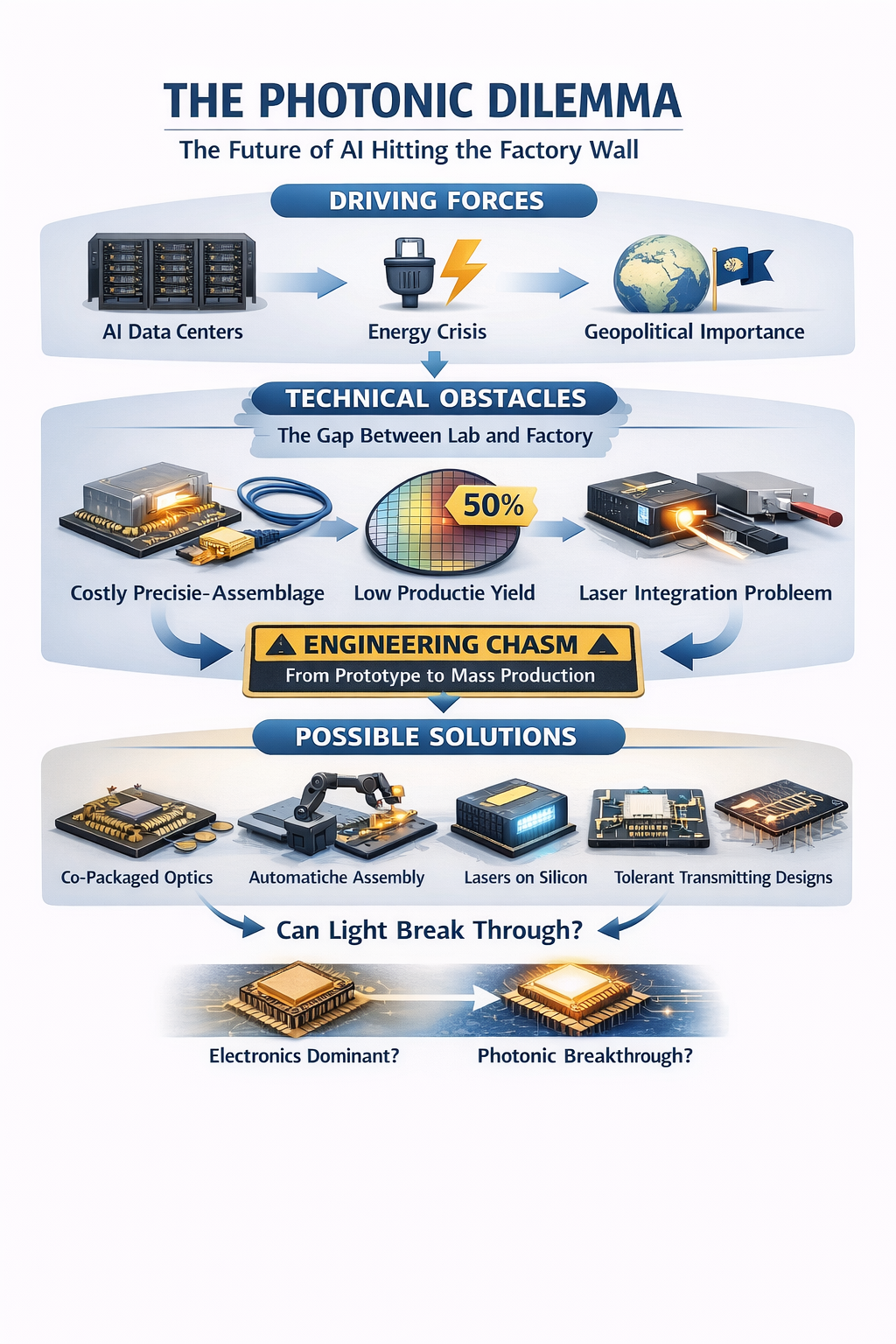
The Engineering Chasm
In laboratories around the world, photonic chips work remarkably well. Researchers have demonstrated optical neural networks, photonic accelerators, and ultra-high-speed optical interconnects. The physics is sound and the prototypes are convincing.
The challenge begins when engineers attempt to manufacture these devices in large quantities.
“The challenge isn’t making one photonic chip that works; it’s making a million of them where the laser alignment doesn’t fail. Photonics is currently where electronics was in the 1950s—moving from discrete components to true integration.”
Pat Gelsinger
CEO, Intel
Source: Intel Foundry Direct Connect
This gap between laboratory success and industrial production is sometimes described as the engineering chasm—the difficult transition from prototype technology to reliable mass manufacturing.
Photonics faces several distinct barriers along this path.
Precision Assembly
Unlike electronic circuits, which tolerate small manufacturing variations, optical systems require extraordinary precision. To transmit light efficiently, optical fibers and lasers must align with photonic waveguides at nanometer scales.
In many current systems, this alignment process still requires active calibration during assembly. Engineers must power the laser, adjust the fiber position microscopically and lock it into place once the signal reaches peak intensity.
This process is slow, expensive and difficult to automate.
As a result, packaging—the process of integrating the chip with lasers, fibers and protective housing—can account for the majority of the cost of photonic systems.
The Yield Problem
Another challenge lies in manufacturing yield.
In traditional semiconductor fabrication, mature CMOS processes can produce chips with yields exceeding ninety percent. Photonic chips, by contrast, are extremely sensitive to microscopic imperfections.
Tiny surface roughness or fabrication defects in optical waveguides can scatter light and degrade performance. Even minor irregularities can turn a functioning device into a defective one.
For complex photonic circuits, yields can drop dramatically—making large-scale production economically challenging.
The Laser Problem
Perhaps the most fundamental obstacle is the integration of the light source itself.
Silicon, the material at the heart of modern electronics, is excellent for guiding light but poor at generating it. As a result, photonic chips often rely on external lasers or hybrid integration with other semiconductor materials.
This hybrid approach introduces additional complexity and manufacturing steps. It also creates new points of failure within the system.
Until engineers can reliably integrate lasers directly into silicon-based manufacturing processes—or develop more efficient hybrid techniques—the scaling of photonic chips will remain difficult.
The Industrial Race
Despite these challenges, industry momentum around silicon photonics is accelerating.
Startups and established semiconductor companies alike are investing heavily in optical interconnect technologies designed specifically for AI infrastructure.
Companies such as Ayar Labs, Lightmatter, Intel and Broadcom are experimenting with new approaches to integrate photonics into existing semiconductor supply chains. Their strategies range from co-packaged optics—placing optical components alongside processors—to automated photonic assembly techniques designed to reduce manufacturing costs.
For these companies, the goal is not simply to build better chips. It is to build a scalable ecosystem capable of supporting the next generation of AI computing.
The stakes are enormous. If optical interconnects become viable at scale, they could fundamentally reshape the architecture of data centers.
A Strategic Technology
The implications extend far beyond the semiconductor industry.
Artificial intelligence is rapidly becoming a strategic technology, influencing economic competitiveness, national security and global technological leadership. The infrastructure required to train and run large AI models is increasingly viewed as critical national capability.
As a result, governments and industry alliances around the world are investing heavily in advanced semiconductor and photonics research.
Silicon photonics sits at the intersection of these efforts. It represents not only a technological frontier but also a potential strategic advantage for countries capable of mastering its manufacturing challenges.
The Future of Light-Based Computing
For now, most experts believe the near future will involve hybrid systems that combine electronic processors with optical interconnects.
In these architectures, traditional GPUs and accelerators will continue performing computations, while photonic technologies handle the increasingly demanding task of moving data between them.
If this hybrid model succeeds, the first widespread deployment of photonic interconnects could appear within the next decade in large-scale AI data centers.
Beyond that horizon lies a more speculative possibility: computing architectures that rely heavily on photonics not only for communication, but for computation itself.
Such systems could potentially unlock new levels of efficiency and performance.
But before that future arrives, the industry must solve a much more mundane problem.
It must learn how to manufacture light.
The Real Race in AI
The history of technology shows that breakthroughs rarely depend on theory alone. Progress emerges when scientific insight meets engineering discipline and industrial scale.
Silicon photonics has already cleared the scientific hurdle.
The next challenge lies on the factory floor.
The race for AI supremacy may ultimately be decided not by software developers or algorithm designers, but by engineers who can transform delicate optical experiments into robust, manufacturable technologies.
In the coming decade, the question facing the industry is deceptively simple: Can light be built at scale?

Figure 1 — The Photonic Dilemma: From Scientific Breakthrough to Manufacturing Challenge
Conceptual map of the silicon photonics value chain for AI infrastructure. While photonic chips promise higher bandwidth and lower power consumption than copper interconnects, the transition from laboratory prototypes to large-scale manufacturing remains difficult. The main bottlenecks lie in laser integration, precision optical alignment and packaging complexity—factors that create what engineers call the “engineering chasm” between research success and industrial deployment.
Graphic credit
Illustration: OpenAI / ChatGPT (conceptual diagram), 2026.
This broader shift—from electrons to photons—is part of a deeper transformation in how we understand intelligence itself: not merely as software, but as something grounded in physics, energy and infrastructure.
In The Age of Light — Meaning, Machines and the Physics of Intelligence, I explore how photonics, energy systems and physical computing architectures are reshaping artificial intelligence—and with it, the balance of technological power in the 21st century.
Available worldwide on Amazon (Kindle Edition):
https://www.amazon.com/dp/B0GMXLX56T