Grenoble’s Photonics Test: Who Shapes the AI Systems Built Around European Chips?
Near Grenoble, silicon photonics is already entering volume production. CEA-Leti is working on what comes next. The distance between those two facts defines Europe’s industrial opportunity.
Europe’s photonics story is often told in the future tense. New pilot lines will open. Start-ups will scale. Optical connections will help AI systems move more data with less energy. Around Grenoble, part of that future has already arrived. The harder question is whether European companies can turn technical and manufacturing strength into influence over the systems their chips serve.
The distinction matters. CEA-Leti develops technologies and processes that industry may be able to manufacture. Nearby in Crolles, STMicroelectronics is already producing its own PIC100 silicon photonics platform on 300 mm wafers for optical connections in data centres and AI clusters. These are separate industrial trajectories, but together they show how much of the photonics challenge has moved beyond the laboratory.
A production contract can bring revenue, technical learning and a stronger position for the next product generation. It does not, by itself, settle who defines the larger AI system.
The next contest is over reliability, capacity, customers and the architecture of the finished system.
A factory, not just a promise
In March 2026, STMicroelectronics announced that PIC100 was entering high-volume production. The platform supports the optical transceivers that carry data between parts of large computing systems. ST says customers have made long-term capacity reservations and plans to more than quadruple production by 2027. That is a stronger commercial signal than a laboratory demonstration: capacity is being expanded against stated customer commitments. It remains a company plan whose delivery will have to be measured over time.
The location matters. ST manufactures PIC100 at its 300 mm facility in Crolles, close to Grenoble. At a moment when Europe is asking how to retain advanced chip production, an established European semiconductor company is already supplying an enabling part of AI infrastructure from a European factory. Its work with Amazon Web Services also puts that production in direct contact with a large buyer rather than leaving it dependent on a hoped-for market.
Yet a production contract answers only part of the strategic question. Hyperscalers decide where optical connections are needed, how modules fit into their networks and which performance requirements suppliers must meet. ST can gain substantial value by meeting those requirements at scale. The wider system may still be specified by the customer.
A European supplier involved early in those decisions can become more than a wafer producer.
That is not a weakness peculiar to ST. It is how much of the semiconductor industry works. But it makes Europe’s claim to industrial power more demanding than the claim that chips are manufactured on European soil.
What CEA-Leti is trying to move
CEA-Leti works further upstream. Its value lies partly in giving new ideas a credible route towards industrial processes. In March, it announced a collaboration with French start-up NcodiN to develop optical interposer technology on a 300 mm integrated photonics process. NcodiN is pursuing very small lasers for optical connections closer to the computing chip, where moving data through conventional electrical links becomes increasingly difficult.
The partnership aims to establish whether that technology can be made compatible with a wafer process suited to commercial scale. It is an industrialisation programme, not an announcement that NcodiN’s interposers are already in mass production.
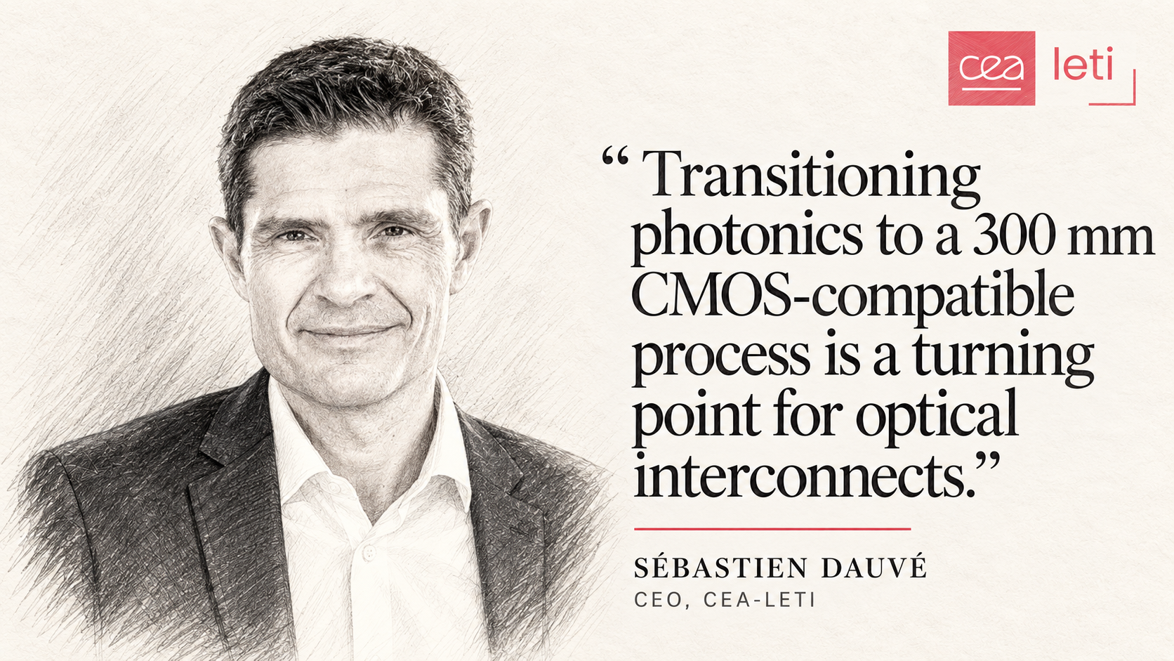
“Transitioning photonics to a 300 mm CMOS-compatible process is a turning point for optical interconnects.”
Sébastien Dauvé, CEO, CEA-Leti, on the collaboration with NcodiN.
The emphasis on process is revealing. A promising optical link must survive repeated fabrication, testing and packaging before a customer can design it into an expensive AI system. Its cost and performance have to remain predictable across wafers and over time. CEA-Leti’s task is to reduce that uncertainty so a manufacturer can eventually take over.
Grenoble therefore represents two different stages at once: established production at ST and industrial process development at CEA-Leti. It would be misleading to present PIC100 as the product of the NcodiN collaboration, or to assume that every CEA-Leti demonstrator will become a European-made commercial chip.
The value of a customer
A European supply chain needs more than research institutes and factories. It needs companies willing to commit to products early enough to shape what gets built.
ST’s position illustrates the opportunity. Its PIC100 roadmap extends beyond current optical modules towards denser integration nearer the processor. Those future products will require choices about packaging, heat, performance and how photonic and electronic components work together. A supplier involved in those choices can become more than a source of wafers. It can help define a product that customers find difficult to replace.
But demand from a global hyperscaler does not automatically produce a European system industry. Europe may secure manufacturing jobs, intellectual property and export revenue while the architecture of AI infrastructure is settled elsewhere. Conversely, access to demanding customers can give a European manufacturer the volumes and feedback needed to improve its technology. The question is how much influence the supplier retains as that relationship deepens.
A place on the wafer is valuable. A place in the architecture is harder to win.
CEA-Leti’s international partnerships make the same issue visible from the research side. In April, CEA-Leti and CEA-List announced work with Taiwan’s PSMC on optical communication and computing technologies for 3D chip systems. Such cooperation can move European research towards practical products. It also means that future manufacturing and system decisions may cross several jurisdictions. A European technology can be valuable worldwide without every stage of its deployment remaining in Europe.
Connecting the European pieces
Grenoble does not have to carry this transition alone. STMicroelectronics leads the European STARLight consortium, which aims to develop 300 mm silicon photonics manufacturing and applications for data centres, telecommunications and other markets through 2028. CEA-Leti is among the research participants. Separately, the European PIXEurope pilot line links capabilities across countries and materials, including design, fabrication, packaging and testing.
Those programmes address a real gap: a chip that works in one laboratory must be usable by designers, transferable to a production process, testable at scale and valuable in a finished product. Shared infrastructure can make that journey easier. It cannot guarantee that a start-up finds customers or that a manufacturer wins a lasting place in a global system.
This is where Grenoble adds something distinct to the discussion about Eindhoven. Eindhoven is building capacity around indium phosphide photonics. Grenoble brings together advanced silicon photonics research and an existing route to commercial production nearby. The two centres do different jobs within a broader European industry. Their strategic value will depend on whether firms can connect those strengths to design tools, packaging, dependable supply and customer commitments.
The evidence from Crolles makes it possible to ask a more precise question than whether Europe can produce photonic chips. It can. CEA-Leti’s work with emerging technologies shows how much remains unsettled about the next generation.
Europe’s test is whether it can repeatedly turn those advances into products that customers adopt at scale, while keeping European companies involved in the decisions that define the system. A place on the wafer is valuable. A place in the architecture is harder to win.
Image credit: AI-generated pencil illustration for Altair Media, based on a Sébastien Dauvé portrait published by Leti Innovation Days. CEA-Leti logo used as a visual reference. Quote from the CEA-Leti–NcodiN announcement, 11 March 2026.
Caption: Sébastien Dauvé, CEO of CEA-Leti. His work on 300 mm photonics points to Grenoble’s larger test: whether European research can become industrial products that European companies help define.
