CEA-Leti Launches Programme to Test Emission Controls for Chip Fabs
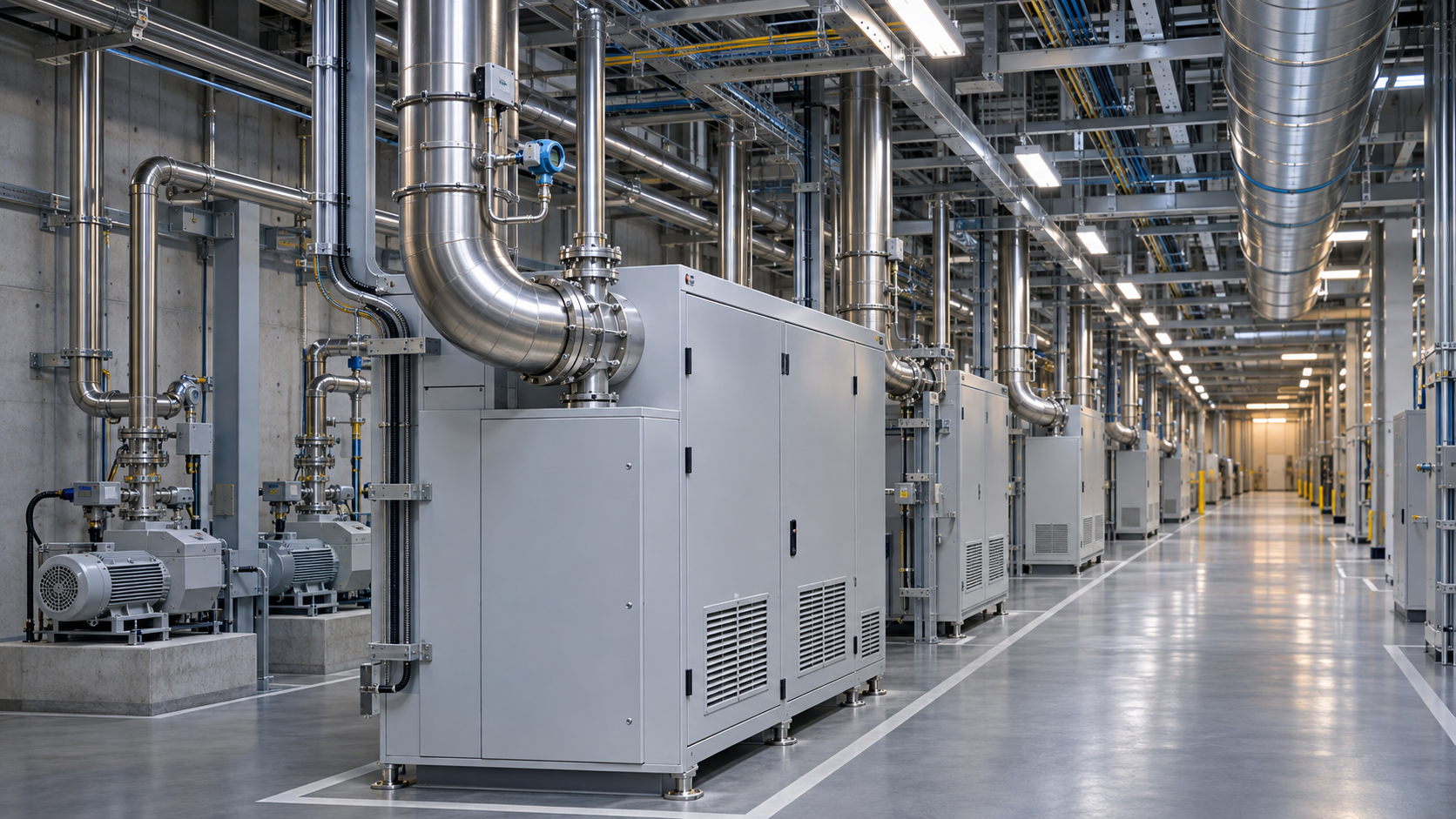
The Grenoble pilot line will track what leaves the cleanroom and test how treatment systems can respond as emissions change.
CEA-Leti and International SubFAB Research Labs (ISRL) launched SubFAB Labs at SEMICON Europa in Munich on Tuesday. The industry-funded programme will test technologies to curb pollution from chipmaking. Work has begun at CEA-Leti’s pilot line in Grenoble, where researchers will measure what manufacturing processes release into exhaust gases and wastewater.
The programme focuses on the subfab, the infrastructure beneath the cleanroom. This is where vacuum pumps draw gases out of production equipment and where systems treat exhaust and wastewater. What reaches those systems depends on what happens upstairs. Etching removes material from a wafer, while deposition adds thin layers. The two processes can generate different by-products, and the compounds present and their concentrations help determine what kind of treatment is needed.
CEA-Leti is running the programme with ISRL, a US company founded by former Intel subfab lead Ilya Zabelinsky. The first phase could run for up to four years. It will build a reference database for participants and develop a monitoring system that combines several kinds of sensors. By running the pilot line under conditions designed to resemble high-volume production, the partners can follow waste streams over months, from the production tool to final treatment.
Among the first partners are HORIBA and TOFWERK, which will test instruments that identify and measure compounds at different points in the waste stream. Edwards Vacuum will study how those streams vary and test whether treatment systems can adjust in real time as the mix of gases changes. The measurements will help suppliers decide which compounds to target and where in the system to intervene.
Further phases are due to begin in 2027. They will cover the treatment of PFAS, often called forever chemicals, as well as emissions and waste from etching, deposition, cleaning and polishing. The work comes as European regulators consider a broader PFAS restriction covering uses in electronics and semiconductor manufacturing.
CEA-Leti plans to assess how much prototype systems reduce emissions and what their operation means for cost, safety and waste handling. A system that removes more of a process gas may also require more water. Both figures matter when a factory decides whether to install it.
A new fab can design its exhaust and wastewater systems around equipment selected before production starts. In an operating fab, a new system has to fit the space and equipment already in place, and installation may have to be scheduled around production. The Grenoble trials will give factory operators data to assess whether the gains measured on a pilot line can be achieved at their own sites.
Caption
Beneath a semiconductor cleanroom, vacuum pumps and pipework carry process gases to treatment equipment. The illustration depicts a typical subfab.
Image credit
AI-generated illustration for Altair Media Europe
