Can Light-Based Computing Learn to Remember?
Eindhoven’s DUAL3M project is developing a missing component for photonic computing. Its industrial promise depends on what the memory can actually do—and who can make it.
Light can move information quickly across a chip. Keeping that information available for the next calculation is harder. Eindhoven University of Technology and Dutch company Motion Imager have begun a project to develop a compact, rewritable memory for future photonic computing systems. The aim is significant. The device, its performance and its path to production still have to be demonstrated.
DUAL3M runs from 2026 through 2030, with budgeted project costs of about €1.06 million. This is an exploratory research programme, working toward a demonstrator that could be integrated into a computing platform. Its central idea is a memory accessible through both light and electricity. That makes the project more specific—and more interesting—than a promise of a fully optical computer.
🟦 What is Eindhoven actually trying to build?
The researchers want to store information in changeable material states rather than hold photons inside a chip indefinitely. Their approach investigates phase-change materials that could retain multiple information levels and be written and read electronically as well as photonically. A TU/e research position describes the intended outcome as a multilevel memory device compatible with electronic and photonic chips. It describes a research objective, not a finished component.
The ambition is a hybrid interface: a place where electronic and photonic parts of a future computer could access the same stored information. Whether it can do that reliably remains to be shown.
🟦 Would it remove the costly conversion between light and electricity?
It could reduce some conversions in a future architecture. If a useful memory state can be set and read optically, a processor would not always need to send an intermediate result through conventional electronic storage. But DUAL3M deliberately retains electronic access too. Its value may lie in combining the two domains effectively, rather than eliminating one of them.
The frequently repeated “1,000 times more energy efficient” claim should not be attached to this project. Its published description gives no measured thousandfold energy improvement for the proposed memory. Speed, switching energy, how long a state lasts and how many times it can be rewritten remain questions for the research.
🟦 Where might the first use appear?
Motion Imager wants the memory to complement the unconventional computing hardware it is developing. It points to real-time modelling in industrial processes, including machining and automated welding, as a possible use for faster, more efficient computing. Those examples explain why the company is involved; they are not announcements of deployed systems or customers for a memory chip.
This is a different starting point from Grenoble’s production of optical interconnects for AI infrastructure. A useful industrial demonstrator could establish a market for the memory before anyone can claim it as a general solution for AI computing. The first test is whether the team can integrate it into a computing platform and measure an advantage on a defined task.
🟦 Who would manufacture it?
For now, TU/e and Motion Imager are the named project partners. Motion Imager says it wants to develop intellectual property for such a memory module within its own hardware programme. The published project information does not name SMART Photonics, another foundry or a commercial production site for the device. Access to Brainport’s photonics expertise is valuable, but access is not a manufacturing agreement.
A production route will depend on the materials, the chip platform, repeatable fabrication and how the memory is packaged with electronic and photonic components. Those choices are part of the industrial question the project must eventually answer.
🟦 What would turn a promising memory into an industry?
A convincing demonstrator would need to show more than the ability to store several states. Those states must remain distinguishable, last long enough for a useful application and survive repeated writing and reading. The next test would be whether a manufacturer can reproduce that performance—and whether a system maker will design a product around it.
Eindhoven already has an industrial story about moving photonic chips from prototype to production. DUAL3M asks a different question: can Europe develop an essential computing function of its own before tomorrow’s architectures are settled elsewhere?
Signal
TU/e and Motion Imager are working on a potential missing component for photonic computing. The breakthrough has yet to be demonstrated. The strategic prize is a memory that can be made reliably, integrated into a useful system and produced at scale.
Image credit
AI-generated illustration for Altair Media.
Caption
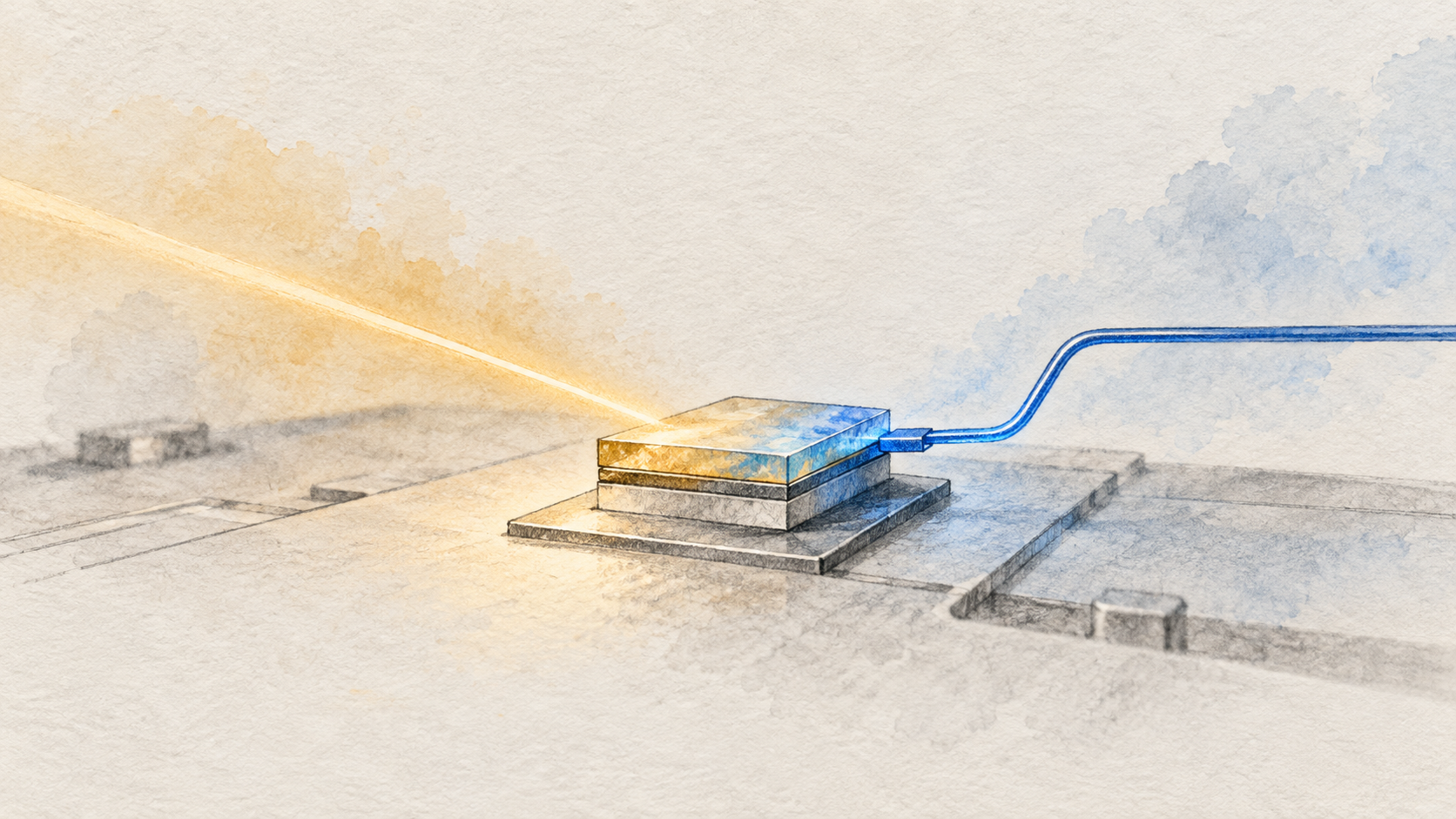
A symbolic view of DUAL3M’s research goal: bringing optical and electronic access together in a future memory device.
